
Thermal Challenges
Understand the engineering problems that make modern
thermal measurements difficult and how each affects
accurate thermal characterization.
Modern thermal measurement runs into the same handful of problems, again and again. Sometimes the material itself is too thin or too small to behave like the bulk. Sometimes the interface between two materials dominates the result more than either material alone. Sometimes heat moves differently depending on direction. Sometimes a manufacturing or growth process shifts the material’s thermal behavior without changing its identity on paper. And sometimes the number that matters isn’t an average at all, it’s what’s happening at one specific location. Most difficult thermal measurements trace back to one or more of these five patterns.
Modern materials aren’t always characterized at room temperature or under ideal laboratory conditions. Laser Thermal systems and lab services support measurements across challenging operating environments, including elevated temperatures, liquids, phase-change materials, and coatings where both thermal conductivity and emissivity influence performance.

Thin Films & Multilayer Structures
When layers become thin enough, conductivity, interfaces, and substrates all begin influencing the measurement.
A conductivity value that matched at one film thickness stops matching once the process shifts and the film comes out thinner, even though nothing about the material itself changed. That’s because thermal conductivity is not a fixed property once a film gets thin enough. A film measured at 200 nm and the same material at 20 nm can report meaningfully different conductivities, and neither number matches the handbook bulk value either. The substrate underneath is not a passive backdrop either; it actively participates in the measured response, and how much of that response belongs to the film versus the substrate is often one of the unknowns.
Multilayer stacks compound this further. Modern devices routinely stack several thin films, each film with its own thickness-dependent conductivity, on top of that substrate. A single bulk measurement can’t resolve which layer is limiting heat flow, it returns one averaged number for a structure that has several independent unknowns, including how much of the signal is coming from the interfaces between those layers rather than the layers themselves. As any individual film gets thinner, its own contribution to the measured signal shrinks while the interfaces bounding it do not, so the thinner the film, the more the measurement is actually describing its boundaries rather than the material itself.
High-conductivity films are one hard edge of this problem. Materials like diamond, GaN, and boron arsenide generate very little measurable temperature rise, pushing signal toward the detection limit, and heat spreads laterally rather than staying confined to a cross-plane path. At high conductivity, interface resistance can dominate the signal entirely, so a measurement intended to capture the film ends up measuring the boundary instead.
Insulative and high-k dielectric films are the other hard edge. Materials like HfO2, Al2O3, and TiO2, grown by atomic layer deposition down to a few nanometers, are now common in CMOS-compatible devices where power dissipation at the nanoscale is a real design constraint. At that thickness, the film is barely thicker than the interfaces bounding it, and separating the two requires resolution most techniques were never built for.
Bulk methods like guarded hot plate, laser flash, and D5470 assume a simple, known structure. They can’t fit a multilayer stack, or resolve a weak high-k signal, or isolate a film only a few atomic layers thick, without collapsing everything into assumptions, and every assumption becomes an error source in the reported conductivity.
Separating a thin film from its interfaces generally takes one of two approaches: measuring a series of the same film at different thicknesses and extracting the film’s own contribution from how resistance scales with thickness, or measuring a very thin reference sample of the same material to establish the interface contribution on its own, then subtracting it from a thicker film’s result.
FASTR resolves individual layer conductivities within a stack using frequency-domain thermoreflectance, fitting multiple unknowns simultaneously rather than assuming them away, and reaches ultra-thin and sub-micron structured films where other techniques run out of resolution. TOPS extends this coverage from thin films through bulk material, using its lock-in thermography method where in-plane behavior matters.

Thermal Interfaces
The interface often determines thermal performance, but conventional measurements usually report only the average.
A material tests fine on its own, and still runs hotter than expected once it’s bonded, coated, or attached to something else. That’s because every interface between two materials carries some thermal boundary resistance, and that resistance often dominates a system’s total thermal budget more than either material’s bulk conductivity. Standard bulk conductivity measurements cannot isolate this resistance either; they report an average across the stack, hiding the interface’s individual contribution.
This becomes critical wherever a bonded joint, adhesive layer, deposited film, or soft interface material sits between two components: TIM pads, gels, and liquid greases in power electronics, die-attach interfaces, bonded semiconductor stacks, coating-to-substrate boundaries. A material can meet its bulk specification and still fail in application because the interface, not the material, is the bottleneck, and for TIMs specifically, that bottleneck can worsen over time as pump-out or dry-out degrades contact through repeated thermal cycling.
Phase-change materials add a further complication: their thermal behavior isn’t fixed at all; it shifts by design as the material moves from solid to viscous to molten with temperature. Characterizing a PCM means capturing performance before, during, and after that transition, not a single steady value, and the interface itself, how well the material wets and contacts the surfaces around it, changes right along with the phase.
As films get thinner, the effect intensifies. Below roughly 50 nm, interface resistance can rival the resistance of the film itself, and conductivity, interface resistance, and heat capacity become coupled in the measured signal. Most techniques have no way to separate them, so the reported number is really the wrong number, an average masquerading as a material property. Because the interfaces themselves don’t shrink as the film does, their share of the total resistance only grows, and in some stacks the interfaces end up accounting for most of what’s measured, with the film itself almost incidental to the result.
Extracting a true value requires characterizing both interfaces independently, the transducer/film boundary and the film/substrate boundary, along with precise film thickness. Any uncertainty in TBR propagates directly into the extracted conductivity.
FASTR resolves this at the micron and sub-micron scale, decoupling both interfaces from an ultra-thin film in a single instrument, including at buried interfaces, with a sensitivity standard methods cannot reach. TOPS addresses the same problem at the material and system scale, characterizing interface performance in soft pads, gels, liquid TIMs, and phase-change materials directly, including through a PCM’s transition.
Anisotropic Materials
When heat moves differently in different directions, one conductivity value is no longer enough.
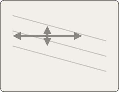
A conductivity number checks out on paper, and the part still doesn’t spread heat the way it should. That’s often because the material doesn’t conduct heat equally in every direction, heat that should be spreading sideways is instead trying to escape straight through, or the reverse, and the number on the datasheet was never describing the direction that actually mattered. This shows up across a range of real materials: graphite sheets, aligned fiber composites, layered crystals, and oriented filler TIMs can show an order of magnitude difference between in-plane and cross-plane conductivity. The effect is especially acute in fin-based and other vertically integrated device architectures, where heat travels through narrow, high-aspect-ratio features and transport becomes strongly directional and sensitive to atomic-scale disorder.
Standard measurement techniques are built around an isotropic assumption. Many resolve only one direction, typically cross-plane, and report it as though it represents the material. For a heat spreader or TIM chosen specifically for its in-plane spreading, that measurement answers the wrong question.
Anisotropy is increasingly something engineered on purpose, not just characterized after the fact. Isotropic TIMs struggle to exceed roughly 10 to 12 Wm-1K-1 without sacrificing mechanical compliance, which has pushed development toward aligned and networked filler systems: oriented graphene, boron nitride, and boron arsenide architectures built specifically for directional conduction. The same push shows up at the thin-film level, where engineered anisotropic films have demonstrated in-plane conductivities rivaling or exceeding some of the best-known thermal conductors. Confirming that an engineered material actually performs the way it was designed requires the same directional sensitivity as characterizing a naturally anisotropic crystal.
Separating the two directions requires sensitivity to each independently, not an average and not an assumption. In most cases this is done on the sample exactly as delivered, either by combining two measurement modes that are each sensitive to a different combination of the two directions and solving for both, or by directly measuring how far heat spreads sideways from a controlled point. Only in the hardest cases, where the in-plane signal is especially weak or a highly conductive substrate overwhelms it, does resolving both directions require engineering the sample itself to force heat down a chosen path.
FASTR resolves in-plane and cross-plane thermal conductivity in ultra-thin and sub-micron structured anisotropic films, including epitaxial and layered materials, where standard geometry alone can’t separate the two directions. TOPS covers the same problem from thin films through bulk material, resolving in-plane behavior directly in composites, TIMs, and other bulk anisotropic materials.
Process-Induced Variability
The same material can perform differently because processing changes its thermal behavior.
Two batches of the same material, same nominal formulation, perform differently once they’re in the field. That’s because thermal conductivity is not a fixed material constant, it’s a process- and structure-dependent property that shifts with dopant concentration, grain size, defect density, growth conditions, or formulation, even when nothing changes on paper. Two wafers of the same material, grown by different methods or doped to different levels, can have meaningfully different thermal conductivity, and a handbook value describes neither.
The mechanism is consistent across material systems: impurities, dislocations, stacking faults, and grain boundaries all increase phonon scattering and reduce conductivity. In doped silicon, conductivity can drop by roughly 22% at dopant concentrations near 2×10¹⁹ cm⁻³ relative to intrinsic material, and similar trends appear in doped GaN and other semiconductor systems. In thin layers below roughly 100 nm, boundary scattering compounds the effect further, suppressing conductivity even at moderate doping levels.
The same principle holds in composites and manufactured materials, just through different levers. Filler loading, dispersion quality, cure profile, sintering conditions, and additive manufacturing parameters all shape the thermal pathways that form inside a material, and a small shift in any of them can change whether a continuous conductive network forms at all. A composite that meets specification in one batch can underperform in the next if a processing step drifted, even though nothing about the formulation changed on paper.
This makes variability a first-order design and reliability concern, not background noise. As growth, doping, and process control have all improved, the achievable spread in thermal properties has widened rather than narrowed, and the relevance of a single reference value has diminished accordingly. A process step that shifts grain structure, defect density, or filler dispersion, whether wafer to wafer or batch to batch, can change effective thermal performance enough to affect device temperature and reliability, without changing the material’s nominal identity at all.
Reference-value measurement can’t catch any of this, because it isn’t designed to. Confirming real performance means measuring the material as grown, doped, processed, and formulated, not as tabulated, at the conditions it will actually see, including elevated operating temperature where that’s part of the application, and doing it across enough sites or batches to characterize the variation itself rather than a single point.
FASTR and TOPS support this directly, with measurement speeds suited to characterizing conductivity across a wafer, a batch, or a set of process conditions, turning variability from an unknown into a controlled, measured parameter soon enough after a process step to still act on the result. FASTR extends this to elevated operating temperature as well, measuring conductivity from room temperature up to 300°C, so performance can be confirmed under the conditions the material will actually see, not just at room temperature.

Localized Thermal Behavior
When thermal performance varies from point to point, average measurements stop answering the real question.
An engineer designs and tests expecting a certain thermal profile, based on a simulation, assumed bulk properties, or a vendor’s datasheet, and the part doesn’t behave that way. Something is running hotter than expected, and there’s no way to tell what’s causing it or where it’s coming from. That’s the same underlying problem whether the original expectation came from a model or an assumption: understanding how heat behaves at specific locations, not as a single averaged number for the whole part.
Single-point bulk measurements can’t resolve either case. A model can’t be corrected against one aggregate value, and a hotspot can’t be located by a technique that reports one number for the entire sample. Both jobs require measuring at the locations that matter, and comparing point to point, not producing a single characterization and hoping it generalizes.
The same non-uniformity shows up in bulk materials with no simulation or device involved at all. Foams, aerogels, and fibrous insulation can vary significantly from point to point due to porosity, density, or fiber orientation, and a single bulk number says nothing about where a material is underperforming or how consistent a batch really is.
This is also where problems invisible from the surface get found. A subsurface defect, void, or delamination can sit beneath a surface that looks completely normal under inspection, at depths conventional techniques with limited penetration can’t reach. Whether the job is resolving a mismatch between simulation and silicon, tracing a failure to a specific process step or region, or finding a defect no inspection caught, the output isn’t a map for its own sake, it’s the answer to where the part is failing or why the model was wrong.
FASTR and TOPS both support spatially resolved measurement, at the resolution and speed needed to move from an averaged number to point-specific answers, whether the goal is validating a model, characterizing a bulk material’s uniformity, or finding a defect no model predicted.
Five Key Challenges for Increasing U.S. Domestic Semiconductor Manufacturing Capacity
As US semiconductor manufacturers work to answer the call for renewed leadership in domestic chip manufacturing, what are the most important challenges that will need to be addressed?
Related Information from Our Learning Center

Overcoming Challenges in Thermal Conductivity Measurement, from Soft TIMs to CVD Diamond

Thermal characterization matters more as AI accelerators intensify an existing package-level bottleneck

Five Key Challenges for Increasing U.S. Domestic Semiconductor Manufacturing Capacity

What is Thermoreflectance?

Unlocking Thermal Measurements in Thin Films

Overcoming Challenges in Thermal Property Measurement and Imaging of TIMs

Thermal Measurements for Emerging Materials – State-of-the-art measurements for thin films, TIMs, and high-temperature materials
Heat Beneath the Surface: Thermal Metrology for Advanced Semiconductor Materials and Architectures

Unveiling Phonon Contributions to Thermal Conductivity and the Applicability of the Wiedemann–Franz Law in Ruthenium and Tungsten Thin Films.
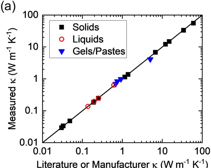
A thermo-optical plane source method to measure thermal conductivity
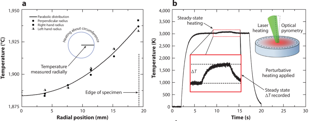
Limitations and Advances in Optical Thermal Transport Measurements: Extremes in Properties, Length Scales, and Temperature
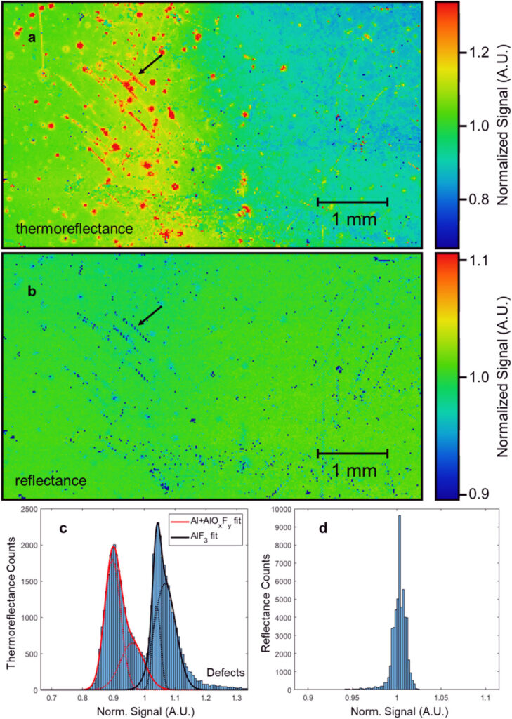
Characterization of AlF3-Passivated Aluminum Mirrors using non-contact thermal metrology
Thermal Conductivity
Thermal Resistance
Specific Heat, Volumetric Heat Capacity, and Thermal Diffusivity
Introduction to Thermal Metrology
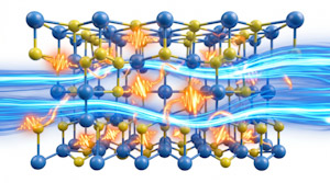
High Thermal Conductivity and Thermal Boundary Conductance of Homoepitaxially Grown Gallium Nitride (GaN) Thin Films
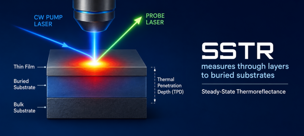
Thermal Conductivity Measurements of Sub-Surface Buried Substrates by Steady-State Thermoreflectance
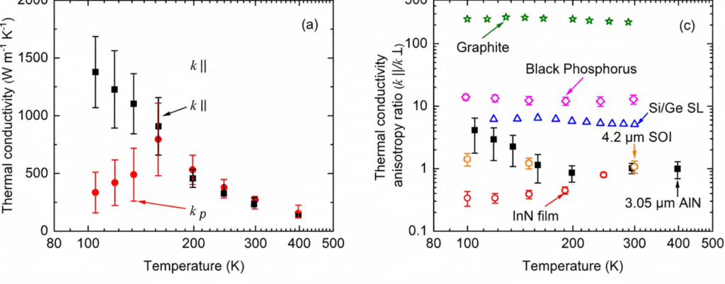
High In-Plane Thermal Conductivity of Aluminum Nitride Thin Films
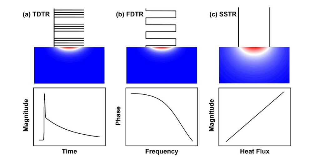
Spatially Resolved Thermoreflectance Techniques for Thermal Conductivity Measurements from the Nanoscale to the Mesoscale
A Steady-State Thermoreflectance Method to Measure Thermal Conductivity

Volumetric Heat Capacity Unit Conversion Calculator
Thermal Conductivity Unit Converter
Temperature Rise Calculators
Thermal Energy Unit Conversion Calculator