Thermal Metrology Instruments
Built for the measurements established methods
were never designed to make.
You’re building materials and architectures that didn’t exist five years ago: films measured in nanometers, stacks where the interface dominates, pastes and liquids that won’t hold a shape. The thermal characterization you need comes from your actual sample, at its actual scale.
Laser Thermal instruments give engineers, researchers, and academic labs these measurements directly. Non-contact and automated from setup to result.
Why Engineers and Researchers Choose Laser Thermal
Every instrument we build, today and in the future, is designed around three commitments. Here is what they mean for your work.
Trust the result, whoever runs the test
A thermal conductivity value is only useful if it holds next week, on the next sample, with the next operator. Alignment, calibration, and data fitting are automated, so results don’t depend on who is at the bench. Put the data straight into a model, a paper, or a qualification report.
Measure what standard methods can’t reach
Established methods were designed for bulk, homogeneous samples, and they still do that job well. Our instruments cover everything else: liquids and liquid metals in place, pastes and gels in their working state, anisotropic materials, and films so thin the thickness changes the physics. You stop designing around what you can’t measure.
Get answers while the design question is still open
Outsourcing every sample adds weeks or months to each design iteration. In-house custom setups build backlogs and depend on the few experts who can run them. Our instruments measure in seconds to minutes per spot and handle sample batches automatically, so thermal data keeps pace with your development cycle.
Find The Right Thermal Instrument
Three questions narrow the choice: what you need to measure, how small your structure is, and what the material is. Most answers point to one instrument. Some point to both, and many labs run them side by side.
What do you need to measure?
- Thermal conductivity of bulk materials, thick films, and coatings: TOPS or FASTR
- In-plane thermal conductivity: FASTR for thin films, TOPS for bulk materials, wafers, and thick films
- Cross-plane thermal conductivity: FASTR. TOPS can also fit it for anisotropic bulk materials
- Effective thermal conductivity of composites and filled materials: TOPS
- Interface thermal resistance (thermal boundary resistance) at bonds and buried layers: FASTR
- Volumetric heat capacity: FASTR
At what length scale are you working?
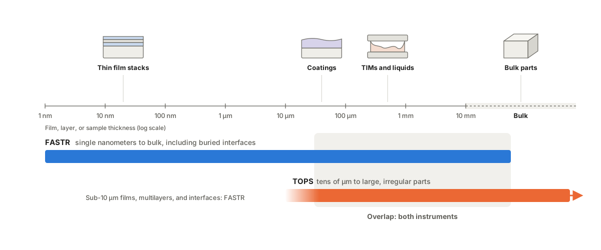
- Single-nanometer to 10 μm films, multilayers, and buried interfaces: FASTR
- Films tens of μm thick, coatings, and bulk parts: TOPS and FASTR (TOPS has no thickness limit and takes large, irregular parts)
- Mapping across a sample from 10 × 10 μm to 150 × 150 mm: FASTR (fine spatial resolution) or TOPS (up to 150 × 150 mm at about 200 μm per pixel)
What material are you testing?
- Thermal interface materials: pastes, gels, gap pads, fillers, and phase change materials: TOPS
- Liquids and liquid metals, measured in place with no compression: TOPS
- Soft, rough, or irregular samples that can’t accept a vacuum-deposited metal layer: TOPS
- Semiconductor wafers, die, thin films, and multilayer stacks with a polished surface: FASTR
- Diamond wafers and heat spreaders: TOPS for in-plane at wafer scale, FASTR for cross-plane near the surface
- Anisotropic materials: TOPS for bulk and thick films, FASTR for thin films
- High-conductivity materials such as diamond, SiC, AlN, and GaN: FASTR and TOPS, up to 3,000+ Wm-1k-1
At a glance
| Attribute / dimension / factor | FASTR | TOPS |
|---|---|---|
| Best for | Thin films, multilayers, interfaces | TIMs, liquids, bulk materials, and films without metal deposition |
| Measures | Thermal conductivity (cross-plane & in-plane), thermal boundary resistances, volumetric heat capacity. | Thermal conductivity, measured directly by steady-state analysis with no heat capacity or density needed. Lock-in analysis adds in-plane sensitivity for anisotropic bulk and thick-film materials. |
| Length scale | Single nanometers to bulk | Tens of μm films to large, irregular bulk parts |
| Thermal conductivity range | 0.05 to 3,000+ Wm-1k-1 | 0.01 to 3,000+ Wm-1k-1 |
| Time per measurement | Under 1 s (SSTR), under 90 s (FDTR) | 5 to 30 s per spot |
| Repeatability | <0.5% dynamic repeatability | ±1% dynamic repeatability |
| Sample surface | Specular, with an 80 nm metal transducer | Rough surfaces accepted, optional removable film |
| Materials | Wafers, die, thin films, multilayer stacks, bulk solids | Thick films, TIMs, gels, pastes, liquids, liquid metals, foams, glasses, bulk solids |
| Temperature | Room temperature to 300 °C | Room temperature |
Our Thermal Metrology Instruments
FASTR
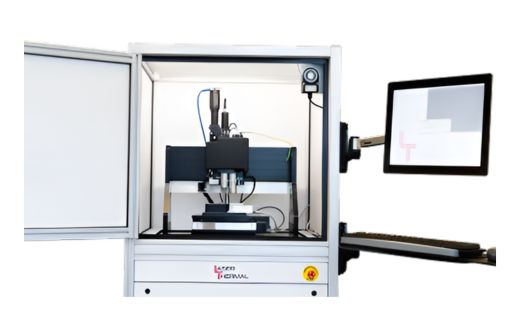
FASTR is the only commercial system that combines frequency-domain and steady-state thermoreflectance (FDTR and SSTR) in one platform. You get the complete thermal picture of a layer stack from one instrument, instead of piecing it together from outside labs or a custom research setup.
Its fiber-coupled design removes the need for optics expertise. New users are running measurements after half a day of training.
Thermal property maps show how conductivity and interface resistance vary across a wafer or die, so you can find the inclusion, defect, or process drift that a single-point measurement averages away.
TOPS
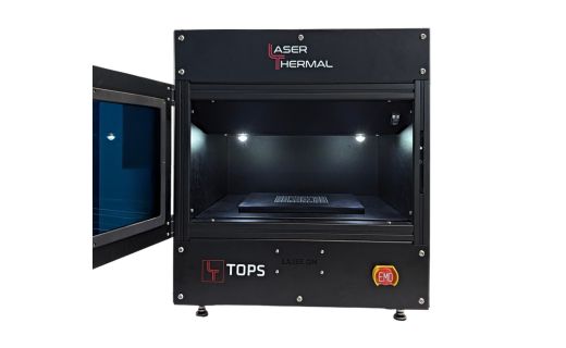
TOPS puts thermal characterization on the bench next to your formulation or inspection work. Measure the finished heat spreader, window, or substrate, not a coupon cut from it. It measures samples in their working state, with no vacuum and no metal deposition, and its removable film transducer lets you recover high-value or limited-quantity samples intact.
Thermal maps show where a TIM spread unevenly or a coating delaminated, so you can fix the process, not just record a number.
For composites and filled materials, TOPS reports an effective thermal conductivity that reflects heat transport through the material, not contact resistance at a test fixture.
From The R&D Bench to The Production Line
A 15% variation in thermal conductivity is interesting in a research sample. On a production line, it’s a yield problem. The measurement that answers a question in your lab is the same one that decides whether a process is controllable at scale.
Our instruments meet thermal questions where they begin: R&D and process development. Our roadmap carries the same measurement toward near-line quality control and in-line production metrology.
- R&D characterization
- Process development
- Near-line quality control
- In-line production metrology
Built On Decades of Thermal Science
Laser Thermal was spun out of the ExSiTE Lab at the University of Virginia. Our founding team has published more than 300 scientific papers, and all R&D and manufacturing happen in Charlottesville, Virginia.
- 300+ publications from the founding team
- 10+ issued or pending patents
- 2024 University of Virginia Invention of the Year
- Recognized by DARPA, the U.S. Air Force, and the Department of Defense
Our Clients Include Industry, Academia, and Government.
The logos below are only those we’re able to share publicly. Our broader customer base includes many of the leading semiconductor fabs, national research laboratories, and power electronics manufacturers driving the industry forward.