
Thermal characterization matters more as AI accelerators intensify an existing package-level bottleneck
Table of Contents
Why the thermal bottleneck moved inside the package
As dies get thinner and substrates and dielectrics shrink to reduce signal path length, the same geometry that helps electrical performance limits how effectively heat can spread. For a growing share of modern chips, the thermal bottleneck isn’t at the lid anymore. It’s at bond lines, underfills, and micro-bump interfaces that were never designed to be a primary thermal path.
That trade-off exists because of how the industry now delivers performance gains. For decades, smaller transistors did the work: faster switching, lower power, with thermal management handled afterward by a heat sink and a fan on a monolithic die. Continued transistor scaling still matters, but on its own it no longer delivers the gains the industry expects. Progress now comes from system-level integration, packing logic, memory, and specialized accelerators closer together than a single die ever could. Imec’s logic technology leadership has argued for several years that continued gains require not just smaller transistors, but better materials, interconnects, and system-level co-optimization working together.
That integration takes two different forms, with very different thermal implications. True 3D logic stacking, placing active compute dies directly on top of one another, is largely solved for memory: HBM stacks and simple cache layers stack vertically today without major thermal issues. Stacking active logic layers is a harder problem. Active logic generates concentrated heat with no direct path to a surface, which is a central reason true 3D logic stacking is still evolving rather than shipping broadly.
The industry’s current workhorse is 2.5D packaging instead. Rather than stacking active chips directly on top of each other, 2.5D places them side by side on a shared, ultra-fine interposer, which sidesteps the worst of 3D stacking’s thermal traps while still delivering the bandwidth AI workloads demand. Every major AI accelerator on the market today relies on some version of this approach: Nvidia’s H100 and Blackwell GPUs, AMD’s Instinct accelerators, and Google’s TPUs are all built on 2.5D interposer packaging, most commonly TSMC’s CoWoS technology. Semiconductor Engineering’s coverage of advanced packaging tracks why even 2.5D isn’t thermally free: shrinking the interposer and dielectrics to reduce signal path length limits how effectively heat spreads laterally across it, which is the same dynamic pushing the bottleneck away from the lid and into the bond lines and interfaces below it.
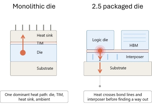
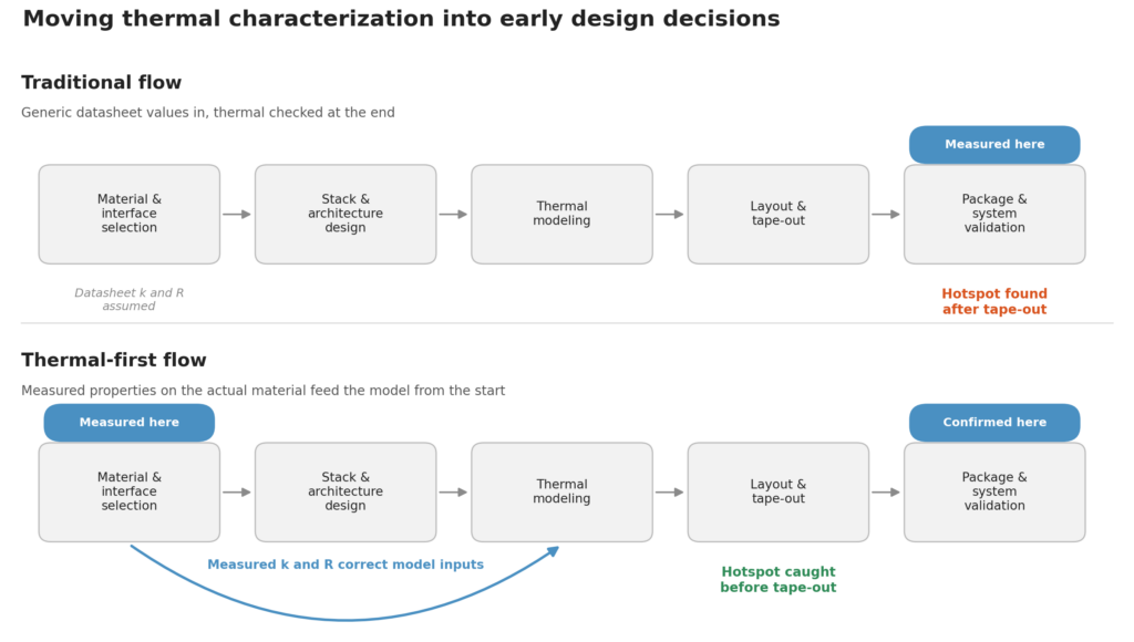
The practical consequence is that thermal considerations can no longer wait until a design is mechanically finalized. When the dominant thermal resistance lives inside the package rather than at its surface, late-stage fixes are architectural, not incremental. A cooling solution bolted on after tape-out cannot compensate for a stack that was never designed with heat flow in mind, which is part of why thermal metrology has moved from a validation step at the end of a program to an input that shapes early architectural decisions.
AI accelerators are rewriting the thermal budget
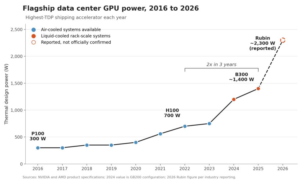
Nowhere is that shift more visible than in AI accelerators and high-performance computing hardware. A decade ago, a flagship data center GPU was rated at 300 watts. By 2022, Nvidia’s H100 had reached 700 watts. Today, Blackwell Ultra parts are rated at roughly 1,400 watts, double Hopper in three years, and next-generation Rubin devices are reported at close to 2,000 watts or more. As die-level heat flux climbs, it is pushing past what air cooling can handle and testing the limits of conventional liquid cooling.
Chipmakers and foundries are responding by moving cooling architecture much closer to the silicon itself. TSMC has demonstrated Direct-to-Silicon Liquid Cooling, which fuses a microfluidic cooling layer directly onto the backside of the die rather than relying on a thermal interface material and a separate cold plate. Presented at the 2025 IEEE Electronic Components and Technology Conference, the approach sustained operation above 2.6 kW of thermal design power on a large multi-die interposer, a level that would overwhelm a conventional lidded package. That is a meaningful signal about where the industry expects power density to go, and it illustrates a broader pattern: cooling is no longer something added after the chip is designed. It is becoming part of the chip and package architecture itself.
A related shift is happening in how power gets delivered to the die in the first place. Backside power delivery, which routes power interconnects beneath the transistor layer instead of above it, frees up routing space for signals and reduces resistive losses, but it also changes where heat is generated relative to the cooling surface. Intel’s PowerVia implementation, one of the first production examples of this approach, delivered a measurable frequency gain alongside reduced power loss. As Intel’s Ben Sell put it, the company’s priority was to fully “understand everything about PowerVia” before combining it with a new transistor architecture, precisely because changes to power delivery ripple into thermal behavior in ways that are easy to underestimate. Every one of these architectural moves, from chiplets to backside power to direct-to-silicon cooling, reinforces the same conclusion: thermal constraints are now a first-order input to system architecture, not a downstream fix.
Why a reference table might not describe your actual device
Engineers modeling a new design will often start with a published thermal conductivity or thermal resistance value for silicon, copper, or whatever interface sits in the stack. That number is a reasonable starting point, but it is frequently wrong for the device actually being built, sometimes by a wide margin.
Thermal conductivity is not a fixed material constant the way some textbooks imply. It depends heavily on how a specific piece of material was grown, doped, and processed. Silicon is a clear example. Introducing boron or phosphorus dopants at concentrations used routinely in device manufacturing disturbs the periodicity of the crystal lattice, which increases phonon scattering and measurably lowers thermal conductivity relative to the undoped material. Foundational thermal conductivity measurements by researchers at Stanford on doped single-crystal silicon films found reductions that scaled directly with impurity concentration, and more recent studies using time-domain thermoreflectance report reductions of roughly 20 percent or more in heavily doped silicon compared to intrinsic material. Film thickness compounds the effect: once a layer drops below roughly a hundred nanometers, boundary scattering starts to dominate regardless of doping level, pulling conductivity further from the bulk reference value.
The same problem shows up in thermal resistance, the property many suppliers list instead of conductivity. Interface and thermal boundary resistance, the resistance to heat flow across a bonded joint or a thermal interface material, depends heavily on bond quality, surface roughness, void content, and cure conditions rather than on the base materials alone. Two interfaces built from nominally identical materials can carry meaningfully different thermal resistance depending on how well they were actually bonded, which is the same process dependence that makes a single tabulated conductivity value unreliable, just showing up in a different property.
Structural details add another layer of variation. Grain boundaries, interfacial roughness, stacking order, and even the specific deposition or growth method used, whether molecular beam epitaxy, chemical vapor deposition, or sintering, all leave a fingerprint on how efficiently a material conducts heat. Two samples with identical nominal chemical composition can behave quite differently depending on the microstructure a given process actually produced. This matters most in narrow, high-aspect-ratio features like fins and vertically stacked interconnects, where heat transport is strongly anisotropic and small variations in growth or processing can shift how heat actually moves through the structure.
The self-heating problem inside individual devices adds a related complication. As one industry expert described it in discussing why self-heating has become harder to ignore at advanced nodes, “all active devices generate heat as carriers move,” and that heat has an increasingly difficult path back out as geometries shrink and vertical integration increases. A single tabulated conductivity or resistance value cannot capture how a specific fin, a specific interface, or a specific doped layer will actually behave once it is fabricated and running under real bias conditions.
None of this means published thermal properties datasheets are useless. It means they should be treated as a starting assumption that thermal characterization on the actual material or interface confirms or corrects, not a fixed input to trust by default. Given how much reliability modeling depends on getting local, junction-level temperature right rather than an average package temperature, an over- or under-estimated conductivity or resistance value doesn’t just introduce noise. It can hide the exact hotspot that determines whether a device survives its expected service life.
The common thread
Taken together, these three shifts point in the same direction. Progress used to come primarily from shrinking transistors, with thermal management handled afterward at the package level. Now, system-level integration, AI-driven power density, and process-dependent material variability all push thermal design earlier into the development cycle and deeper into the physical stack. Treating thermal behavior as something to check late, using generic property values and an external heat sink, is a good way to discover a hotspot after tape-out rather than before it. The engineering teams navigating this well are the ones building thermal assumptions, and the measurements that validate them, into the design process from the start rather than bolting them on at the end.
Further reading:
- Navigating heat in advanced packaging: Semiconductor Engineering
- Self-heating issues spread: Semiconductor Engineering
- Intel is all-in on backside power delivery: IEEE Spectrum
- TSMC’s direct-to-silicon liquid cooling: Techovedas, covering TSMC’s 2025 IEEE ECTC demonstration
- Nvidia Blackwell B200 power specifications: TweakTown
- Thermal conduction in doped single-crystal silicon films: Stanford Nanoheat Lab (Asheghi et al.)
If a datasheet value is the only thing standing between your design and a hotspot you didn’t plan for, it’s worth measuring the material you’re actually building with. Laser Thermal works with engineering teams to characterize thermal conductivity, interfacial resistance, and thin-film thermal behavior directly on production materials, rather than relying on a bulk reference value that may not describe the part in front of you. Contact Us