Contract Testing Services:
Thermal Characterization
Engineering Answers for Your Most Challenging Thermal Questions
As materials, interfaces, and device architectures become increasingly complex, thermal performance can no longer be understood through bulk measurements alone.
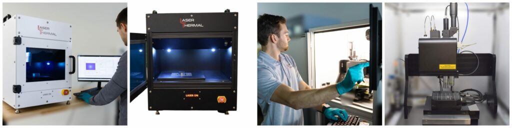
Laser Thermal partners with engineering teams to measure thermal conductivity, thermal diffusivity, and interface resistance in thin films, anisotropic materials, semiconductor devices, thermal interface materials, and aerospace components. Measurements are performed on platforms built specifically for these material classes, not adapted from general-purpose lab equipment.
Whether you need answers for a single project or ongoing development, our engineers recommend the measurement approach best suited to your application.
Trusted by engineers from
The logos below are only those we’re able to share publicly. Our broader customer base includes many of the leading semiconductor fabs, national research laboratories, and power electronics manufacturers driving the industry forward.









What Challenges Are You Trying to Solve?

My simulation does not match reality
Measure real thermal properties for more accurate modeling.

I need to measure or compare candidate materials
Generate reliable thermal data for material selection.

I suspect an interface bottleneck
Characterize thermal resistance across bonded interfaces.

I need to validate a new manufacturing process
Determine whether thermal performance changed after fabrication.

I need data for customers or publications
Produce defensible measurements with detailed reporting.

I don’t know what measurement approach I need
We’ll recommend the appropriate approach.
What Can We Measure?
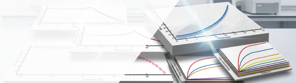
Laser Thermal measures thermal conductivity, thermal diffusivity, and thermal boundary resistance across materials ranging from sub-micron thin films to bulk solids, liquids, pastes, coatings, and complex assemblies. Many of our techniques use one-sided, non-contact optical measurements, making them well suited for valuable prototypes and enabling most measurements to be performed non-destructively. These approaches are also particularly effective for characterizing heterogeneous and anisotropic materials.
The appropriate measurement technique and achievable measurement range depend on your material, geometry, thickness, thermal conductivity, and engineering question. This range is possible because our platforms, FASTR and TOPS, were designed around these material classes directly, rather than extending general-purpose instruments to cover them. Our team evaluates each project and recommends the measurement approach best suited to your application. If you believe your material is outside of a certain property range, please still contact us as we are continuously pushing the limits of our instruments.
| Property | Measurement Range |
|---|---|
| Thermal conductivity (in-plane, cross-plane) | 0.01 to 3,000+ Wm-1K-1 |
| Thermal boundary resistance | >1 m2KGW-1 |
| Thermal resistance | Could span many orders of magnitude based on the actual combinations of thickness and conductivity |
| Thermal diffusivity | >0.0025 mm²/s |
| Volumetric heat capacity | 1 MJm-3K-1 to 4 MJm-3K-1 |
| Thermal property mapping | 10×10 μm to 150×150 mm |
| Emissivity | Spectral range 0.5 μm to 40 μm |
| Melting temperature | Room temperature to 4,000 oC |
Standard lead time: 2-3 weeks from receipt of sample. A 3-day expedited turnaround is available for a surcharge.
Materials and Applications
Thin Films

Thermal Interface Materials (TIMs)

Thermal Insulation Products

Coatings

Bulk substrates and samples

Metals & Alloys

Liquids, Gels & Pastes
Why Teams Choose Laser Thermal For Thermal Characterization Services?
Trusted by leading R&D and manufacturing teams

Proprietary thermal platforms

Thermal metrology specialists
- Application-driven thermal testing is our only focus; we run measurements every day.
- Experienced team in test design and interpretation from micro to macro length scales; we recommend the right method for your questions, not force-fit a tool.

Fast, reliable results
- Rapid turnaround with high-confidence data, clear deliverables, and documented assumptions.
- Consistent and streamlined workflows backed by decades of experience; results you can trust and share internally or with customers.
How Thermal Testing Services Work
Step 01
Consult
Discuss your application, review sample fit, get a measurement recommendation.
Step 02
Propose
NDA, scoped proposal, and quote.
Step 03
Test
Ship samples, measurements performed.
Step 04
Report
Receive your engineering report, discuss results with our engineers.
Frequently Asked Questions About Our Testing Services
Most solid materials, coatings, thin films, interfaces, and assemblies — including production parts, not just idealized test coupons. Our non-contact approach means minimal sample preparation and no destruction of the sample. If you’re not sure your sample is a fit, send us the details and we’ll tell you directly.
Yes. NDAs are handled during the proposal stage, before samples are shipped or specifics are shared. Not every project requires one but we’ll let you know if it’s relevant to yours.
Yes, this is part of the consultation. Tell us your material, geometry, and the engineering question you’re trying to answer, and we’ll recommend the appropriate approach rather than fitting your project to a specific tool.
No. Most customers come to us with a question, not a technique. We’ll match the method to your application
Yes. FASTR characterizes thermal properties of thin films from nanometer to micrometer thickness, using FDTR and SSTR together on the same spot rather than relying on a single spec-sheet number. Lateral resolution is down to 2µm, with feature detection down to 100 nm achievable under sufficient thermal contrast
Yes. Interface resistance across bonded materials is one of the most common reasons customers come to us, since bulk properties alone don’t reveal what’s happening at the bond line. Our approach measures thermal resistance directly across the interface, non-destructively and without requiring the sample to be altered for testing. This applies to TIMs, die-attach layers, bonded stacks, and other multilayer assemblies where the interface itself is the unknown.
Minimum sample dimensions and quantities will depend on the measurements you need and your sample. In general, most samples require: minimum lateral size is 5×5 mm, minimal thickness is 200 nm (very thin films), 20 μm (thin films) or 2 mm for bulk, minimum volume is 22 mL for pastes/gels and 50 ml for liquids.
Standard turnaround is 2–3 weeks, with expedited options available for time-sensitive projects.
Yes. Our methodology and data have been used in peer-reviewed and academic contexts, including work with institutions like NIST.
Our report includes documented assumptions, methodology, plots, uncertainty bounds, analyzed results and recommendations.